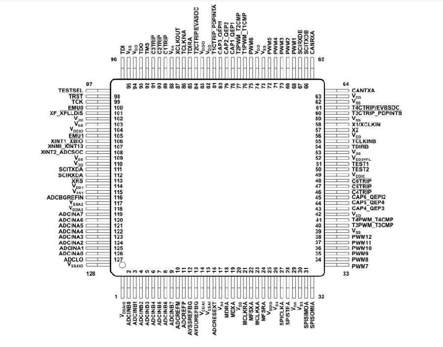
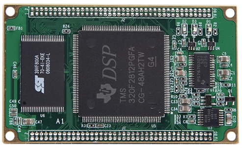
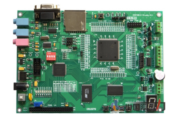
The speed has taken a quantum leap from the TMS320LF2407A, from a maximum of 40M to 150M on the TMS320F2812, and the number of data bits processed has jumped from 16 to 32 bit fixed point. The biggest highlight is its EVA and EVB event managers and the accompanying 12-bit, 16-channel AD data acquisition, which makes it easy to control motors. Coupled with a wealth of peripheral interfaces, such as CAN, SCI, etc., it has a good share in the industrial control field.
TMS320F2812 is a new high-performance 32-bit fixed-point digital signal processor based on the code-compatible C28x core, whose code is compatible with the F24x/LF240x series DSP code and some of the functions, the C28x core instruction execution cycle reached 6.67ns, the maximum operating frequency can reach 150MHz, to ensure that the control system has sufficient computing power This ensures that the control system has sufficient computing power. In addition, the F2812 integrates a number of peripherals to provide a complete on-chip system, reducing system costs and enabling simpler, more efficient control. Its on-chip peripherals mainly include 2 x 8 12-bit ADCs (with the fastest 80ns conversion time), 2 x SCI, 1 x SPI, 1 x McBSP, 1 x eCAN interface, etc. It also comes with two event management modules (EVA, EVB), including 6 x PWM/CMP, 2 x QEP, 3 x CAP, 2 x 16-bit timers (or TxPWM/TxCMP ). In addition, the device has three independent 32-bit CPU timers, and up to 56 independently programmable GPIO pins. The F2812 differs from the F24xx family of DSPs in that it uses a unified addressing approach.

The chip has an internal SARAM of 18K, including MO, M1, L0, L1 and H0, a total of five memory blocks. Each memory block is kept independent, allowing access to different RAM blocks in the same machine cycle, thus reducing pipeline latency. Moreover, the F2812 has 128K words of internal FLASH with address space 3D8000h to 3F7FFFh, which is suitable for low-power and high-performance control systems. In addition, the F2812 provides an external memory expansion interface (XINTF), convenient for system expansion, its addressing space can reach 1MB. F2812 has a variety of power-on boot options, you can set the different states of GPIOF4, GPIOF12, GPIOF3, GPIOF2 for DSP power-on program boot control.
DSP2812 is the new powerful 32-bit fixed-point DSP of TMS320F2812 launched by TI, which is the upgraded version of TMS320LF2407A, the most important feature is that the speed has a qualitative leap than TMS320LF2407A, from the highest 40M to 150M of TMS320F2812, and the number of data bits processed has also jumped from 16-bit fixed-point to 32-bit fixed-point. The number of data bits processed has also jumped from 16 to 32 fixed points. The biggest highlight is its EVA and EVB event managers and the accompanying 12-bit, 16-channel AD data acquisition, which makes it easy to control motors. Together with rich peripheral interfaces such as CAN, SCI, etc., it has a good share in the industrial control field. TMS320F28335 digital signal processor is the latest 32-bit floating point DSP controller from TI. Compared with the TMS320F2812 fixed-point DSP, the TMS320F28335 adds a single-precision floating-point unit (FPU) and high-precision PWM, and doubles the Flash (256K x 16Bit), while adding a DMA function that allows ADC conversion results to be directly stored in any of the DSP's storage spaces. It also adds a CAN communication module, SCI interface and SPI interface. The TMS320F28355 has a main frequency of up to 150MHz and also features an external memory expansion interface, watchdog, three timers, 18 PWM outputs and a 16-channel 12-bit AD converter.
The F28335 has a similar XINTF (External Interface External Interface) to the 2812 but is more powerful, being 16/32 bit data bit width configurable and DMA controllable. This interface allows for easy expansion of off-chip memory and other peripherals during system design and independent setting of their control, which is important for the control of power electronic current converters today. The scalability of the F28335 is a step up from that of the F2808.
The 28335 and 2812 are part of the same C2000 family, the main difference being that the 28335 hardware supports floating point operations and offers superior performance in handling floating point numbers. At the same time PWM, eCAP, eQEP and especially PWM can be controlled separately for each way. The main thing is fixed floating point, 283XX or 2803X are floating point chip, 28XX are fixed point, other functional modules bus what the C2000 is much the same, even the register configuration are similar.
DSP2812 is the abbreviation of the DSP chip TMS320F2812 launched by TI. This CPU chip has a high cost performance, widely used in industrial control, especially the processing speed, processing accuracy in the field of higher requirements, in the field of electronic control plays an important role. The main features of this chip are.

Fast processing speed, up to 150MHz;
On-chip SRAM, Flash;
External memory interface, externally expandable up to 1M*16b storage space;
Numerous external devices, such as SCI, SPI, CAN, EV, ADC, etc.;
A large number of controllable GPIO ports for easy control of external devices.
The external interface (XINTF) is an important interface for the DSP2812 to communicate with external devices. These external interfaces correspond to a certain memory space of the CPU, and the CPU controls the external interfaces indirectly by reading and writing to the memory space. The external interfaces are usually used to expand SRAM, Flash, ADC, etc.
In the DSP2812, the external interfaces are mapped to five fixed memory space zones - Zone (0, 1, 2, 6, 7), each with a chip select signal, and each memory zone can be independently set for access timing.
The signal lines of the external interface are mainly the chip select signal lines (XZCS0AND1, XZCS2, XZCS6AND7), the 16 data buses (XD(15:0)), the 19 address buses (XA(18:0)), the read/write enable signal lines and other signal lines.
In the DSp2812, there are five regions corresponding to five chip select signals, but two pairs of regions share a chip select signal each: region 0 and region 1 share XZCS0AND1, and region 6 and region 7 share XZCS6AND7. For these shared regions, they can be designed as one memory space or external logic can be used to generate two addressing spaces according to actual requirements.

The five regions share 19 address buses and 16 data buses. Depending on the number of data buses and address buses, an external region corresponds to a maximum external addressing space of 512K*16b.
Based on the above information, each region is accessed using a reasonable logic to prevent access conflicts.
Area 0 and Area 1
Region 0 and region 1 share XZCS0AND1, but the address bus of the two regions is different, region 0 uses an address bus of 0x2000~0x3FFF, region 1 uses an address bus of 0x4000~0x5FFF, so the following logic can be used to distinguish between the two regions.
TMS320F2812 is a new high-performance 32-bit fixed-point digital signal processor based on the code-compatible C28x core, whose code is compatible with the F24x/LF240x series DSP code and some functions, the C28x core instruction execution cycle reaches 6.67ns, the maximum operating frequency can reach 150MHz, to ensure that the control system has sufficient computing power This ensures that the control system has sufficient computing power. In addition, the F2812 integrates a number of peripherals to provide a complete on-chip system, reducing system costs and enabling simpler, more efficient control. Its on-chip peripherals mainly include 2 x 8 12-bit ADCs (with the fastest 80ns conversion time), 2 x SCI, 1 x SPI, 1 x McBSP, 1 x eCAN interface, etc. It also comes with two event management modules (EVA, EVB), including 6 x PWM/CMP, 2 x QEP, 3 x CAP, 2 x 16-bit timers (or TxPWM/TxCMP ). In addition, the device has three independent 32-bit CPU timers, and up to 56 independently programmable GPIO pins. The F2812 differs from the F24xx family of DSPs in that it uses a unified addressing approach. The chip has an internal SARAM of 18K, including MO, M1, L0, L1 and H0, a total of five memory blocks. Each memory block is kept independent, allowing access to different RAM blocks in the same machine cycle, thus reducing pipeline latency. Moreover, the F2812 has 128K words of internal FLASH with address space 3D8000h to 3F7FFFh, which is suitable for low-power and high-performance control systems. In addition, the F2812 provides an external memory expansion interface (XINTF) for easy system expansion, and its addressing space can reach 1MB. The F2812 has a variety of power-on boot methods to choose from, and the DSP can be controlled by setting the different states of GPIOF4, GPIOF12, GPIOF3 and GPIOF2 for program boot during power-on.

